
For years,
the electron beam has been essential for semiconductor manufacturing tasks, such as inspection and mask writing.
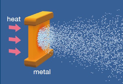
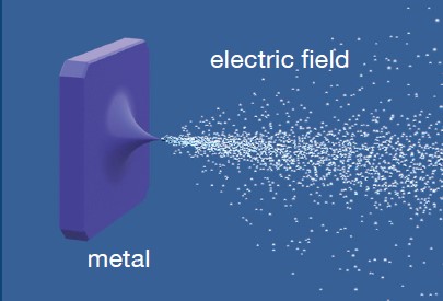
However, the technology has not changed over almost 50 years.Its history can be traced back to the thermal emitter of the 1940s.In the 1970s, the high performance field emitter was developed.
However, as technological innovations in the semiconductor industry accelerated much faster than expected, the requirement for further performance improvement of the electron beam also increased significantly.
We, Photo electron Soul Inc.,
provide solutions for performance improvement based on semiconductor photocathode technology.


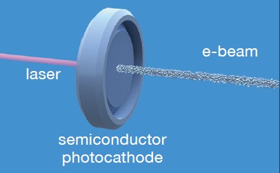
A semiconductor photocathode electron beam is generated by the laser irradiation of special semiconductor materials. Such a beam offers high performance and unique features that have NOT been realized using electron beams in the past.
Despite the advantages, semiconductor photocathode e-beam technology has not been used in industry because the conventional system is massive and complicated.
Photo electron Soul Inc. has integrated all the component technologies, such as semiconductor, vacuum, and optics technologies, by leveraging research accumulated at Nagoya University over 30 years. We have successfully packaged these technologies into small equipment units. This is something no one has ever achieved.
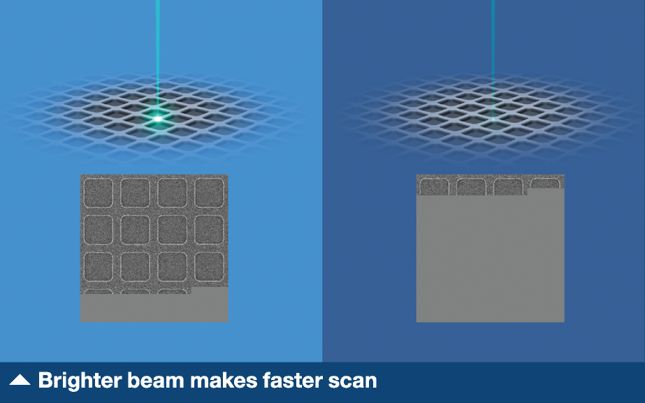
Brighter beam
Our product enables you to generate an electron beam with high current despite extremely low energy dispersion. These levels cannot be produced by the conventional electron beams. We make scanning with a brighter beam possible and reduce the inspection time by accelerating the scanning drastically.
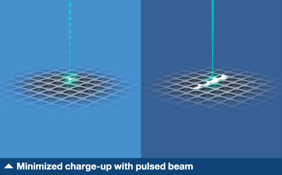
Less charge-up by pulsed beam
Our product can generate a pulsed beam without any complicated system. You only need to switch the continuous laser into pulses to obtain a pulsed electron beam.
Charge-up is the one of the biggest issues faced during electron beam inspection. Our product will reduce charge-up drastically.
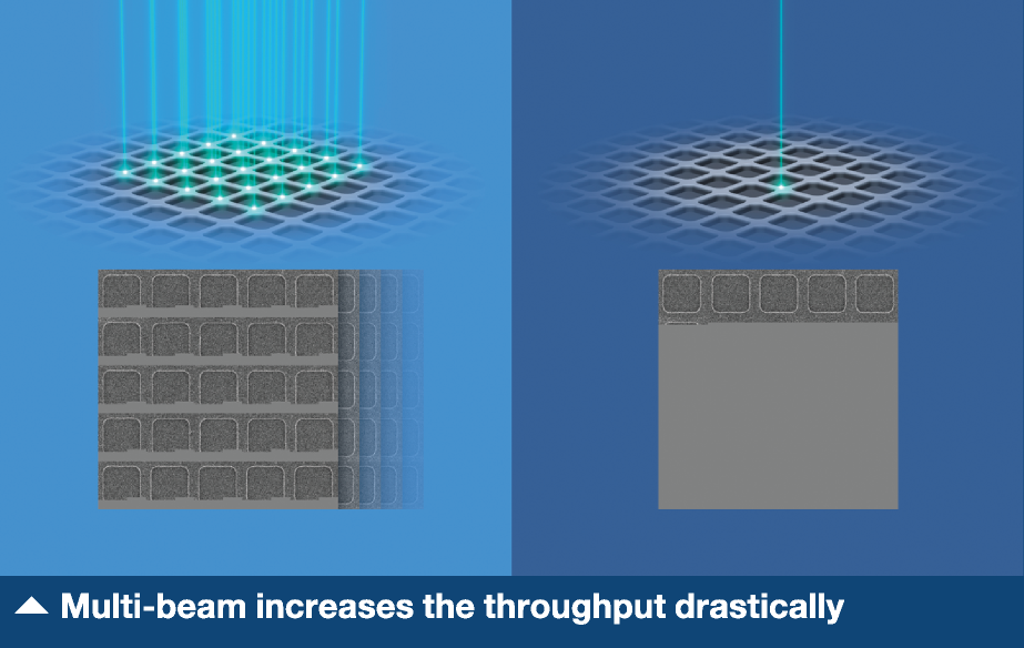
Multi-beam
We can simply extend the product to realize multi-beam capability comparable to the current technologies, such as multi-gun, multi-column, and MEMS splitting.
You can get generate a multi-beam by irradiating the photocathode with multiple lasers.
For inspections, the multi-beam permits simultaneous imaging, increasing the throughput drastically.